بسم الله
After covering the cache in the previous article, today we wrap up the memory topics so we come away with a clear understanding of memory in general — without descending into external memory, which benefits those working directly with hardware more than software people.
Internal Memory
Internal memory is also known as Main Memory:
It represents the memory layers closest and fastest to the processor, used to store data and instructions currently being processed, distinguished by fast random access during operation. It includes the registers, cache, RAM, and ROM.
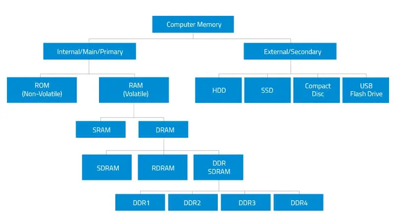 Figure (1): Where internal memory sits
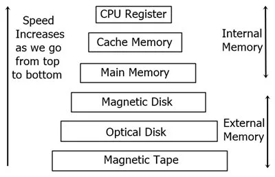 Figure (2): Components of internal memory
Semiconductor Main Memory
Semiconductor main memory refers to the physical memory chips (such as an external DRAM chip) used as the operating system’s primary storage unit. It is memory manufactured with semiconductor technology.
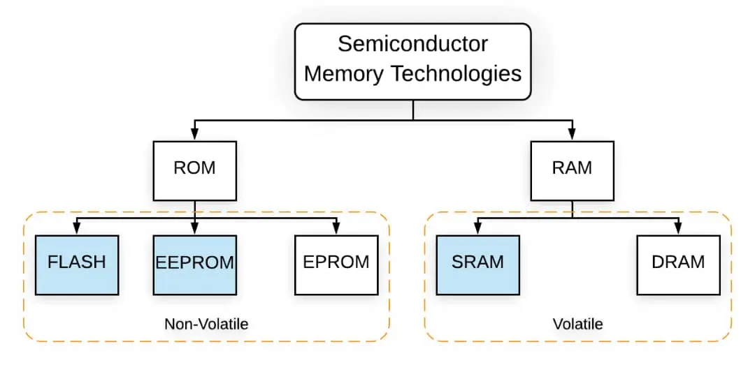 Figure (3): The main memory chip
Before We Start: The Transistor and the Capacitor
To properly understand what follows we need to know the transistor and capacitor. This is outside our main subject, but a surface look suffices:
The Transistor: one of the most important modern electronic components:
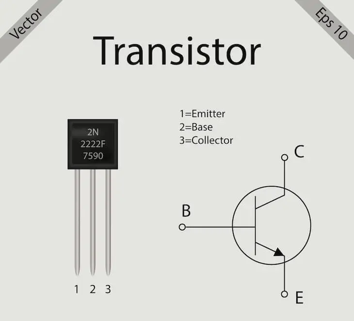 Figure (4): Transistor symbol
Its importance lies in performing two main functions:
- Amplification: boosting weak electrical signals (like audio from a microphone or radio signals). This function does not concern us much here — it matters most to communications people.
- Switching — and this is what we must understand: it acts as an electronic switch controlling current flow through a circuit (on/off). When a small voltage is applied to one of its terminals (the Gate in a MOSFET or Base in a BJT), the transistor passes or cuts a large current between its other two terminals. You can expand further into transistor types.
The Capacitor: briefly, its job is storing electrical energy as charge for a short time and controlling current flow according to signal frequency — like a tiny battery that stores and releases energy instantaneously:
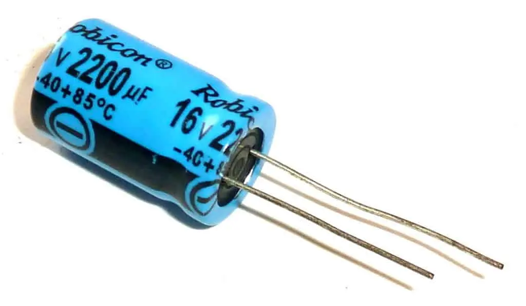 Figure (5): The capacitor
Now Let Us Begin: What Are DRAM and SRAM?
Dynamic RAM (DRAM): A type of volatile semiconductor RAM where each data bit is stored in a memory cell made of one transistor and one capacitor:
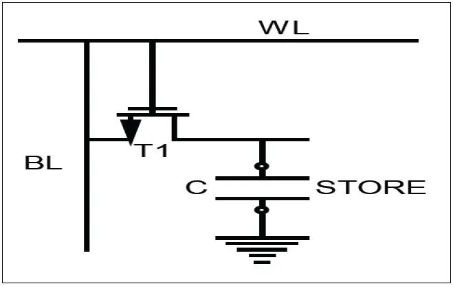 Figure (6): A DRAM cell
The capacitor can be charged or discharged to represent the binary value (0 or 1). But there is a problem: electric charge leaks away over time! It must therefore be refreshed periodically to preserve the data — making DRAM a volatile memory that loses its contents when power is cut.
Thanks to the simplicity of the DRAM cell — just a capacitor and transistor — billions of cells can be fabricated on a single die, yielding high density and low cost per bit.
Static RAM (SRAM): Uses cells built on flip-flop circuits of 4–6 transistors to store each bit:
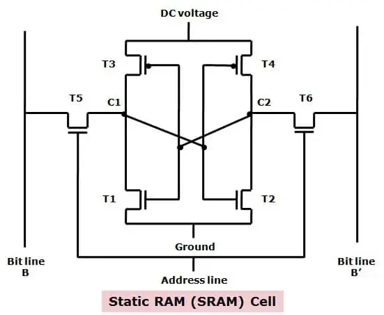 Figure (7): An SRAM cell
An SRAM cell holds its data as long as power is connected, with no periodic refresh needed — hence it is very fast compared to DRAM. But using many transistors per cell means lower density and a higher price. So SRAM serves high-performance roles such as cache and registers, while DRAM fills the primary memory role (RAM):
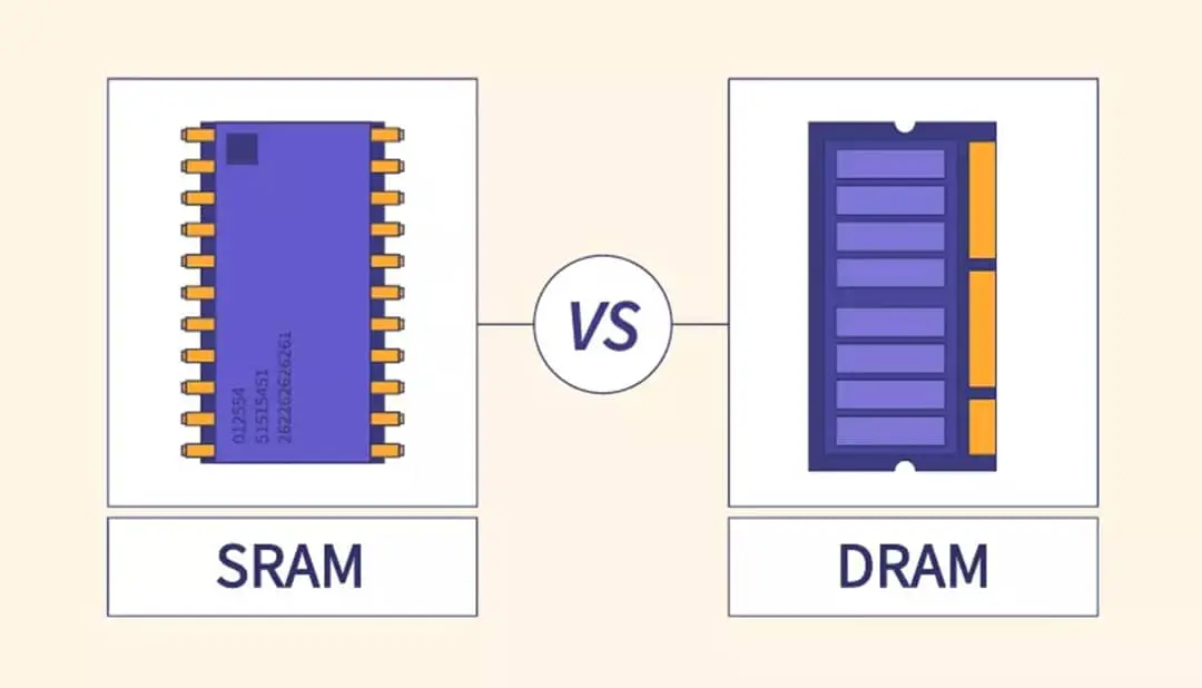 Figure (8): Where SRAM lives
Here is an SRAM vs DRAM comparison:
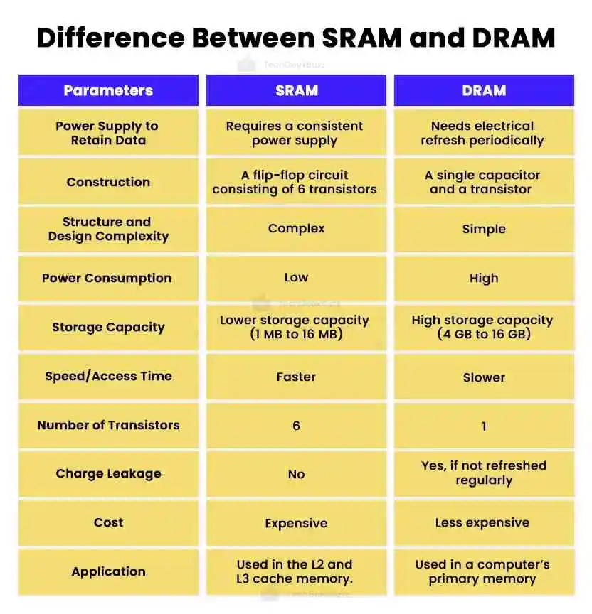 Figure (9): SRAM vs DRAM
All the memories discussed above are volatile.
Non-Volatile Memory
This category covers every memory technology that retains data without power — unlike DRAM and SRAM.
Flash Memory: Flash is non-volatile chip-based memory that can be electrically erased and reprogrammed while preserving data without power:
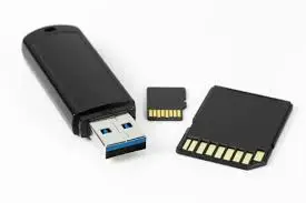 Figure (10): Flash memory types
It splits into two kinds whose names derive from the same logic gates:
- NOR Flash: allows fast random access to individual addresses, suiting it for storing executable code in embedded systems.
- NAND Flash: reads and writes sequential blocks of data (pages) at high speed.
Flash is used in USB sticks, SD cards, and SSD drives. Its read time beats a traditional EEPROM chip, though its write and erase operations remain far slower than reads.
Ferroelectric RAM – FRAM:
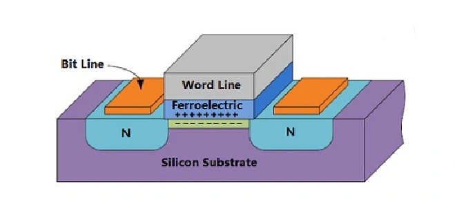 Figure (11): An FRAM cell
It relies on ferroelectric materials structured like DRAM (capacitor + transistor), but uses a special crystalline metal-oxide layer (such as PZT — lead zirconate titanate). That layer keeps its electric polarization after the causing field is removed, which is why FRAM preserves its data without power. It has extremely fast write times and enormous write endurance — published figures range between 10¹⁰ and 10¹⁴ write cycles. It is typically used in applications needing frequent reliable writes: smart cards, power meters, medical devices, and industrial control.
Resistive RAM – ReRAM:
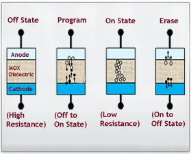 Figure (12): A ReRAM cell
It works by changing the resistance of a solid oxide layer (such as a metal oxide) by generating oxygen vacancies under an electric field. Each cell acts as a variable resistance representing either 0 or 1. This technology is still in development stages — as of this writing.
MRAM & PCM Techniques
Magnetoresistive RAM – MRAM:
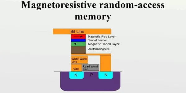 Figure (13): An MRAM cell
MRAM stores bits in magnetic elements called Magnetic Tunnel Junctions (MTJ). A cell consists of two magnetic layers separated by a thin insulating barrier: the fixed layer’s magnetic orientation stays constant, while the other layer (the free layer) can be flipped by a current or an external magnetic field.
The bit is inferred by measuring the junction’s resistance: parallel orientations lower the resistance (‘1’), antiparallel orientations raise it (‘0’). MRAM combines SRAM-like speed with DRAM-like density and is non-volatile.
It also withstands enormous numbers of writes — trillions of cycles (10¹² and beyond) — without meaningful wear. MRAM appears in specialized applications such as aerospace equipment, industrial systems, and buffers. Unlike flash, MRAM can write randomly without erasing a whole page first, giving it better performance under repeated operations.
Phase-Change Memory – PCM:
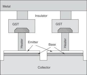 Figure (14): A PCM cell
Data is stored in chalcogenide glass layers. The cell thermally switches between a crystalline low-resistance state (‘1’) and an amorphous high-resistance state (‘0’) by passing a current pulse that generates enough heat to change phase.
PCM is non-volatile with read times faster than classic NAND flash, but needs more energy for writes due to the thermal switching. Its most famous commercial attempt was Intel/Micron’s (Optane, or 3D XPoint).
Memory Arrays
So how are digital memories designed, and what do they contain?
All digital memories rest on arrays of cells organized in rows and columns. A typical memory chip (such as SRAM or DRAM) contains:
- A memory cell at every row/column intersection.
- An Address Decoder selecting the row to read.
- Write Drivers to store data.
- Sense Amplifiers to measure the cell’s signal.
During manufacturing these arrays are built with advanced CMOS processes, and the industry is moving toward 3D stacking to raise capacity — for example, HBM (High-Bandwidth Memory) is made from several layers of DRAM dies stacked on top of each other.
What Should You Take From This Article?
This article builds your general knowledge of internal memory. Focus well on SRAM, DRAM, and Flash, with an appreciation of the remaining technologies — we aim to build a generation capable of learning anything, starting from understanding the computer’s fundamental technologies.
Articles on Digital Systems are coming that will greatly help you understand these techniques, God willing.
I ask God to bless our knowledge and work — keep us in your prayers.