بسم الله
In the previous article we talked about computer architecture and organization and the basic parts of a computer. Today, God willing, we dive a little deeper into the processor itself: its components, its functions, and how they work together.
Data Path & Control Unit
The processor consists of fundamental units:
- The Arithmetic Logic Unit (ALU), which performs arithmetic and logic operations.
- The Control Unit (CU), which generates the control signals needed to coordinate the components.
- Plus a set of fast-access registers.
These components divide into two main parts:
• Data Path: The collection of components responsible for moving and processing data inside the processor. It includes the ALU, the registers, and the data-carrying buses.
Example: processing data involves steps such as moving numbers from memory into registers, performing an addition or subtraction in the ALU, then storing the result in another register.
• Control Unit (CU): Interprets the current instruction and generates the control signals required to execute it (such as read/write signals for registers and memory, and selecting which operation the ALU performs).
Instruction Pipeline
Modern processors execute instruction cycles in a synchronized and parallel fashion through a technique known as the Instruction Pipeline to boost performance; the fetch and decode stages of a new instruction can begin before the final processing of the previous instruction has finished.
So how did this evolution happen, and what changed? The idea revolves around Bus Organization — and if you have looked at networking topologies, you may already have a picture of what is going on.
Single-Bus Organization
Early simple processors relied on a single bus shared by all components (the general-purpose registers, the program counter PC, the instruction register IR, etc.). A single bus can move data between registers and memory, but only one value travels per cycle. All registers — PC, IR, the Memory Address Register (MAR), the Memory Data Register (MDR) — connect to the same bus, and since one bus cannot carry more than one value at the same moment, data transfer slows down.
Two-Bus Organization
This was improved by using more than one bus: with a two-bus organization the processor can, for example, read two values from two registers at the same time, reducing the number of cycles needed and speeding up transfer and execution.
This is what you find in modern processors — and not just two buses: the number of internal buses varies by design, and each core has its own data path and its own buses.
Example:
int a = 5, b = 3;
int c = a + b;
The processor executes this in steps: loading 5 and 3 into two registers (say eax and ebx on x86), then performing the addition in the ALU. The instructions might be:
mov  eax, 5      ; load the constant 5 into EAX
mov  ebx, 3      ; load the constant 3 into EBX
add  eax, ebx    ; the ALU adds eax and ebx, result in eax (so c = 8)
Register Organization
Registers are very small, extremely fast storage inside the processor, used to hold intermediate values, memory addresses, and results. They come in several kinds:
• Program Counter (PC): Holds the address of the next instruction to execute.
• Instruction Register (IR) / Current Instruction Register (CIR): Carries a copy of the currently executing instruction so the processor can decode it and determine its function.
• Memory Address Register (MAR): Holds addresses in memory during fetch and store operations.
• Memory Data Register (MDR) / Memory Buffer Register (MBR): Carries data read from memory or waiting to be written to it.
• General Purpose Registers:
Registers used by the compiler or programmer to hold temporary values while programs run; their count and capabilities vary between architectures. On x86, for example, you find registers such as eax, ebx, ecx, and edx, each 32 bits wide.
What distinguishes these registers is that you can use the whole register or just part of it in operations: EAX is made of 32 bits, split into two 16-bit halves, each of which splits further into two 8-bit sections. Here is an illustrative image:
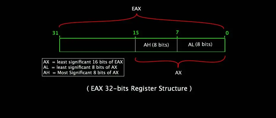 Figure (1): The subdivisions of EAX on x86
What matters here is that register organization design covers: their count, their size (bit width), how they are accessed (read/write), and their purpose.
Example: writing this in C:
int a = 4, b = 5;
might look like this on x86:
mov  eax, 4      ; store the value 4 in EAX
mov  ebx, 5      ; store the value 5 in EBX
Instruction Cycle — Detailed
In the previous article we saw that the instruction cycle passes through three fundamental stages (fetch, decode, execute) — but sometimes two more operations join them:
- Memory Access.
- Write Back.
Let us expand on each:
• Fetch: The cycle starts by moving the current instruction address from the PC into the MAR. The processor asks memory to read the instruction at that address, and the result lands in the MDR. The instruction then moves into the IR to be interpreted. Finally, PC updates to point at the next instruction — either incremented by the instruction’s size, or replaced outright for jumps.
• Decode: With the instruction loaded into IR, the Control Unit analyzes it to determine the operation type and the registers or memory locations involved. The CU sends control signals that define the source and destination of the data (which registers to use, whether memory access is needed, and which operation the ALU should perform).
• Execute: Here the required arithmetic or logic operation takes place in the ALU; for an addition or subtraction, the ALU reads the values from the source registers and produces the result. In general, the ALU performs its operations according to the opcodes carried in the instruction.
• Memory Access: If the operation requires loading data from memory or storing data into it (like load/store instructions), this is the stage where it happens, using the address computed by the ALU to reach memory.
• Write Back: Finally, the result of the operation is written to its proper destination: for an arithmetic instruction, the ALU’s output goes into the target register; for a load-type instruction, the data fetched from memory moves into the register. With that, the instruction cycle completes and the data stands ready for the following instructions.
Example
Suppose we have this x86 assembly code:
mov  eax, 5
mov  ebx, 2
sub  eax, ebx
Let us walk through the first instruction step by step:
- Fetch: the processor takes the first instruction’s address from PC, reads it from memory, and it lands in IR.
- Decode: the CU interprets the instruction in IR as “move the value 5 into eax” and sets up the control signals to write that value into eax.
- Execute: this instruction needs no complex ALU operation (it may simply be treated as an immediate load); the value 5 is passed along, prepared for writing.
- Write Back: the value 5 is actually written into eax.
Notice we never needed the Memory Access stage, since the instruction does not touch memory.
The cycle then repeats for mov ebx, 2. As for sub eax, ebx, this is where the ALU steps in: it reads both values from eax and ebx, produces the difference (3), and the result is written back into eax.
With that, you have seen how the components inside the processor are organized and how instructions flow through them — see you in the next lesson, God willing.
Keep us in your prayers.